![]() Nikon Museum Nikon Museum Special Exhibition
Special Exhibition
Dates: April 3, 2018 (Tue) - June 30, 2018 (Sat)
Reprinted from Nikon's website
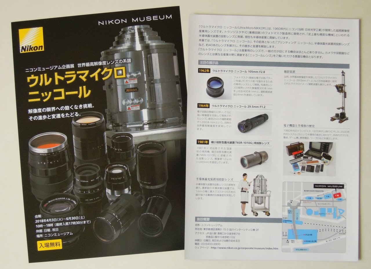
![]() Museum Leaflet Gatecrash the Nikon Museum
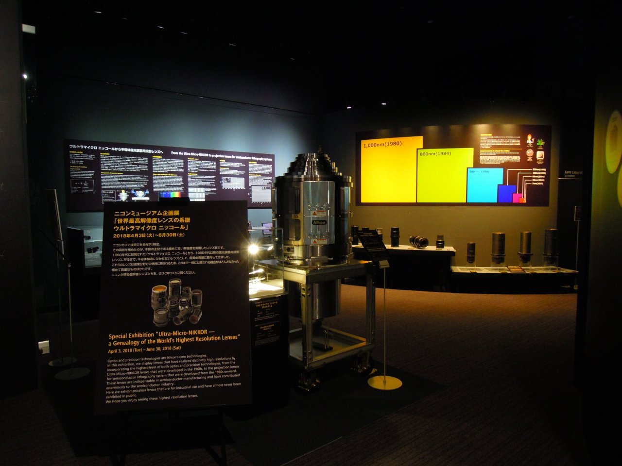
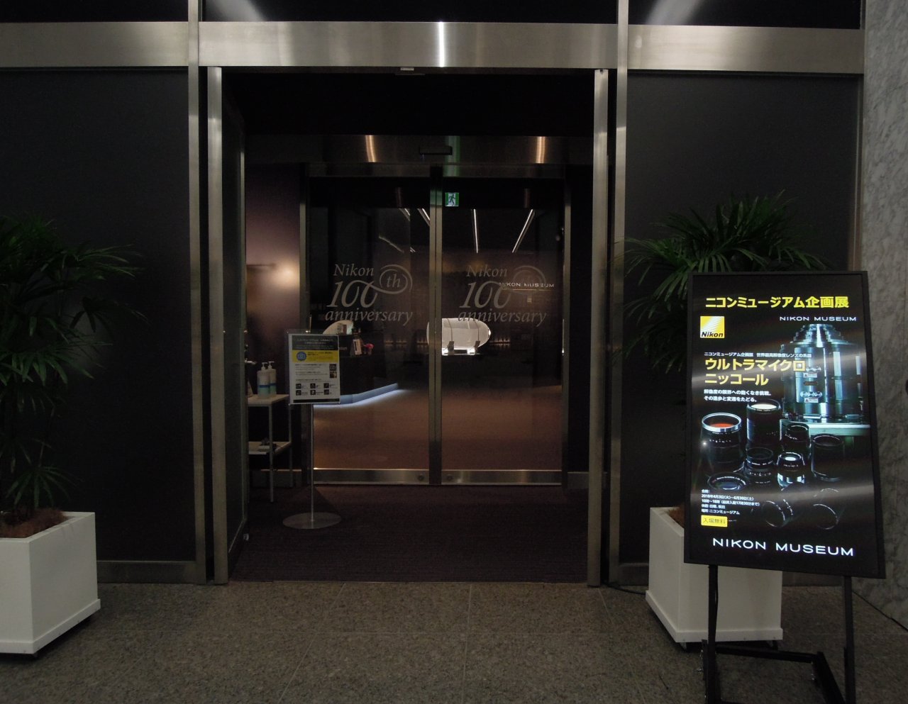
I visited the Nikon museum on 3th April of the opening date of the special exhibition.
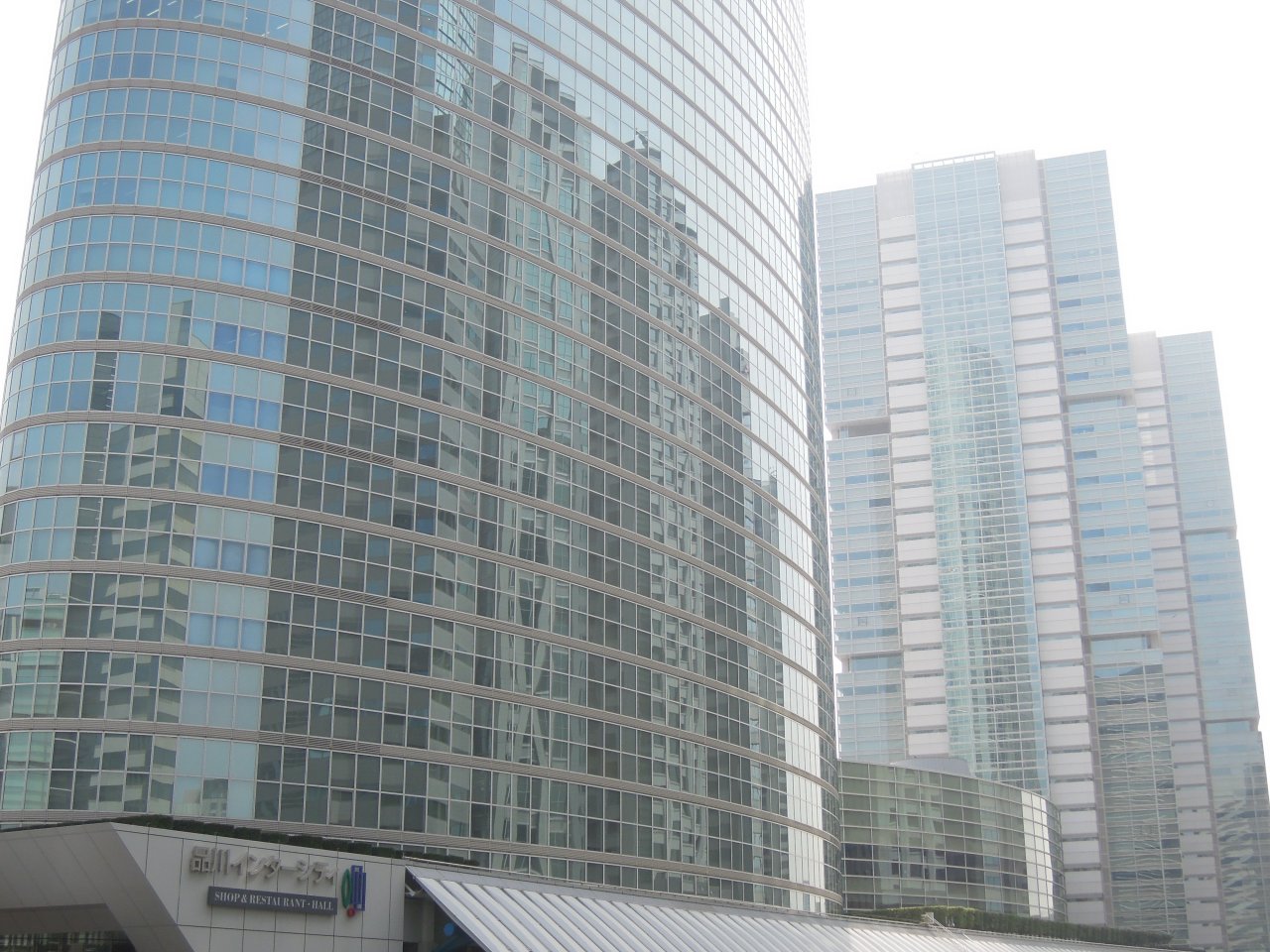
![]() Nikon Headquarters, Shinagawa Tokyo
Sakura Hanami Season Nippon
Gatecrash the Nikon Museum A Genealogy of the World's Highest Resolution Lenses Ultra-Micro-NIKKOR lenses were developed in 1960s by Nikon (then Nippon Kogaku K.K.) especially for use in the production of transistors and ICs. They evolved into projection lenses for semiconductor lithography systems, considered "the most precise equipment in history", and contribute greatly to the semiconductor industry. About 40 lenses are on display in this exhibition, including Ultra-Micro-NIKKOR lenses, their forerunners the Printing NIKKOR lenses, and projection lenses for semiconductor lithography systems, illustrating the progress and evolution of such lenses.
Notes:
![]() A Genealogy of the World's Highest Resolution Lenses
![]() Projection Lens for the NSR-S306C Semiconductor Lithography System, 2001
![]()
Ultra-Micro-NIKKOR 30mm F1.2 Ultra-Micro-NIKKOR Historical Family Trees
![]() Ultra-Micro-NIKKOR Historical Family Trees
![]() What is the Ultra-Micro-NIKKOR Ultra-Micro-NIKKOR
In 1961, Nikon started developing a high-resolution lens at the
request of printing companies and electrical manufacturers.
This lens was used in the production of photomasks for semiconductor
manufacturing.
As a reseult of Nikon receiving a large number of
orders for this lens from overseas as well as Japanese manufacturers,
a series of ultra-high resolution lenses wwas developed named "Ultra-Micro-NIKKOR",
which eventually dominated the world market.
![]() Ultra-Micro-NIKKOR 12mm F1.2 Prototype, 1972
![]() Ultra-Micro-NIKKOR Prototype 28mm F1.5 and 28mm F1.7, 1972
![]() Ultra-Micro-NIKKOR 22mm F1.5 Prototype, 1973
![]() Ultra-Micro-NIKKOR 58mm F1.8 Prototype
![]() Ultra-Micro-NIKKOR 28mm F1.8, 1967
![]() Nikon 1 J5 and UMN 28mm F1.8
![]() Ultra-Micro-NIKKOR 50mm F1.8 for h-line and e-line, 1969
![]() Ultra-Micro-NIKKOR 165mm F4 and 12mm F1.2 Prototype, 1970
![]() Ultra-Micro-NIKKOR 12mm F1.2 Prototype, 1970
![]() Ultra-Micro-NIKKOR 105mm F2.8 (1962) and 125mm F2.8 Prototype (1965)
![]() Ultra-Micro-NIKKOR 55mm F2 and 155mm F4 Prototype, 1965
![]() Ultra-Micro-NIKKOR 155mm F4, 1966
![]() Very Rare e-line Filter 72mm and 40.5mm
![]() Ultra-Micro-NIKKOR 105mm F2.8, 1962
![]() Ultra-Micro-NIKKOR 125mm F2.8 Prototype, 1965
![]() Ultra-Micro-NIKKOR 135mm F4 for g-line Prototype, 1968
![]() Ultra-Micro-NIKKOR 55mm F2 for h-line, 1965
![]() Ultra-Micro-NIKKOR 28mm F1.8, 1967
![]() Professor Dr. Zyun Koana's Micro Dot, 1964 Printing NIKKOR Printing NIKKOR lens was developed to create film duplicates of original movies for screening. It provides high resolution images with superior chromatic aberration and distotion correction, and was also used for the inspection and measurement of minute patterns.
![]() Printing NIKKOR 105mm F2.8 Prototype
![]() Printing NIKKOR 95mm F2.8 Prototype and 105mm F2.8 Lens performance testing system Lens performance testing system is also exhibited, including the system for testing the Ultra-Micro-NIKKOR 29.5mm F1.2 lens, which had the world's highest resolution at the time of its launch in 1964.
![]() A photographic system that demonstrated the world's highest resolution This is a photographic system for macro imaging that was used by Professor Dr. Zyun Koana (1907 - 1985) to demonstrate the performance of high-resolution lenses, including the Ultra-Micro-NIKKOR. A variety of lenses can be used by switching adapters.
The lens attached to the system is the prototype No. 5043 of the Ultra-Micro-NIKKOR 19.5mm F1.2,
which was developed in 1964. The Ultra-Micro-NIKKOR 19.5mm F1.2 achieved a resolution of 1,260 lines/mm in an imaging area of 2 mm, the highest in the world at that time.
![]() Ultra-Micro-NIKKOR 29.5mm F1.2, N0. 5043
![]() A photographic system that demonstrated the world's highest resolution
![]() Big Ultra-Micro-NIKKOR Lenses
![]() Ultra-Micro-NIKKOR 250mm F1.0, 1967
![]() Ultra-Micro-NIKKOR 225mm F1.0, 1967
![]() Ultra-Micro-NIKKOR 225mm F1.4, 1969
![]() Ultra-Micro-NIKKOR 225mm F1.4 and 300mm F1.4, 1969
![]() Ultra-Micro-NIKKOR 300mm F1.4, 1969
![]() Ultra-Micro-NIKKOR 225mm F1.0 Prototype, 1969
![]() Ultra-Micro-NIKKOR 250mm F4, 1971 Reduction Projection Lenses for Semiconductor Lithography System
The Ultra-Micro-NIKKOR evolved into a projection lens for semiconductor lithography systems,
providing both high resolution and a wide foeld of view.
It contributed to the development of the Nikon NSR series, the world's leading lithography system
in semiconductor fabrication.
![]() Reduction projection lenses for semiconductor lithography system
![]() Reduction projection lens for semiconductor lithography system
![]() Projection Lens (for NSR-1010G), 1980
![]() Projection Lens (for NSR-1505G2A), 1984
![]() Projection Lens (for NSR-0510G), 1986
![]() Projection Lens (for NSR-1505G4D), 1987 The History of Electronic Devices and Semiconductors
Furthermore, under the corner title "The History of Electronic Devices and Semiconductors",
radios, calculators, game machines, mobile phones,
word processors and other devices that developed alongside such semiconductors
as the transistors produced in the 1960s,
ICs and LSIs in the 1970s and system LSIs in the 2000s are displayed.
![]() The History of Electronic Devices and Semiconductors 1960 - 1970's
![]() The History of Electronic Devices and Semiconductors 1980's
![]() The History of Electronic Devices and Semiconductors 1990's
![]() Tamagotchi 1996
![]() Thank you !! Nikon Museum Tokyo Special Links
My friend Mr. Siroyagi-san's flickr is great!
His nice blog is here. (Japanese)
Mr. Makoto Suzuki's Special Report, Digi-Came Watch (Japanese) Important Note The father of the Ultra Micro Nikkor lenses is Professor Dr. Zyun Koana of the University of Tokyo. The spelling of his correct name is Zyun Koana. The spelling of Jun koana is incorrect. The spelling of the explanation panel at this exhibition was wrong. The spelling of his correct name is Zyun Koana. ![]()
Copyright Michio Akiyama, Tokyo Japan 2018, 2019
|